
|
SLiC/MP Architecture
Crafting High Performance Desktop Multi-Processing Systems Based on the SLiC/MP™ Architecture
SLiC/MP Abstract
As the number of applications with high computational demands increases, so does the need for more processing power. Applications ranging from CAD/CAM to multimedia are demanding more performance from the underlying systems and microprocessors. Microprocessor architectures and technologies have advanced rapidly in the past few years in order to enable system manufacturers to achieve the system performance levels needed. Microprocessor architectural techniques, such as Superscalar and Superpipelining, are increasing system performance by exploiting instruction-level concurrency, found in most applications, and increasing CPU clock frequency. However, these architectural advances are increasing the manufacturing burden due to the tremendous increase in complexities. An alternative solution to achieving the system performance required is to increase performance by thread-level concurrency or developing Multi-Processing systems.
Multi-Processor (MP) systems achieve higher performance by allowing multiple processors to operate concurrently. This concurrency is achieved on thread, or task level, as opposed to instruction level. Due to that difference, MP systems require more sophisticated operating systems and applications in order to fully exploit the thread-level concurrency. The Windows NT operating system achieves that by being multi-threaded in addition to being MP-ready.
Other MP operating systems are also becoming multi-threaded and MP-ready as well. This trend, in most operating systems, will ensure that MP systems as well as subsequent applications can achieve the performance levels needed without major technological advances in microprocessor semiconductor technology. This does not imply, however, that MP systems will be prevalent unless the cost of developing MP systems is reduces.
The new generation of microprocessors is enabling the development of lower cost MP systems by taking into account the MP system requirements during the microprocessor development phase. These architectural advances reduce much of the traditional hardware overhead associated with developing an MP system and optimize for performance, software compatibility and cost.
This paper discusses an open MP architecture, designed by Cyrix, called SLiC/MP™ that can be used to craft high performance MP desktop systems.
| CPU Architecture | Cache-to-Cache Transfers | Write Allocate | Summary | Page Top | Introduction to the SLiC/MP Architecture The SLiC/MP™ architecture is a high performance desktop MP system architecture that offers PC compatibility and symmetric MP support and is suitable for next generation desktop MP systems.
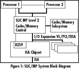 Figure 1 illustrates a typical desktop MP system utilizing SLiC/MP. The SLiC/MP architecture is optimized for systems that use a shared second level cache and cache controller. Traditionally, MP systems used a private cache for every CPU element at a cost premium. The SLiC/MP architecture, on the other hand, enables the development of high performance MP systems at a lower cost. This is due to many architectural enhancements that address both bus bandwidth and interrupt handling. Microprocessors utilizing the SLiC/MP architecture will have optimized first level cache architecture that achieves a high cache hit rate. In addition, processors will contain additional MP-specific features that minimize bus traffic (increasing available processor bus bandwidth), as well as reduce processor bus latencies. SLiC/MP also specifies a high performance interrupt control architecture that is optimized for desktop Multi-Processor systems and achieves 100% PC compatibility. A key aspect of the interrupt architecture is its compatibility with processors from different processor vendors. SLiC/MP Interrupt architecture is intended to be an open solution that supports various desktop MP implementations, CISC or RISC based, without restrictions.
| CPU Architecture | Cache-to-Cache Transfers | Write Allocate | Summary | Page Top | SLiC/MP Interrupt Architecture The SLiC/MP interrupt architecture achieves high performance, PC compatibility and low cost by optimizing for the key components in a Symmetric Multi-Processor (SMP) operating system environment. SMP systems require that all processors have equal access to system resources, such as memory and input/output (I/O) devices. In addition, SMP systems require a mechanism that enables processing elements to communicate among one another. This form of communication is referred to as Inter-Processor-Interrupts (IPIs). Communication is needed to ensure system coherency and coordination. The SLiC/MP interrupt architecture is a key component in ensuring symmetry between the processing elements and providing a high performance communication channel between the processing elements.
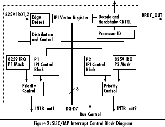 Figure 2 illustrates the SLiC/MP interrupt control block diagram. This control module is intended to be part of the cache control component of a SLiC/MP-compliant system. Integrating this control module will enable off-the-shelf uniprocessor cache controllers to become SMP-ready and SLiC/MP compliant. In addition, the SLiC/MP architecture achieves high performance at a very low cost compared to other solutions.
| CPU Architecture | Cache-to-Cache Transfers | Write Allocate | Summary | Page Top | SLiC/MP System Interrupt Control The SLiC/MP architecture is fully compatible with the PC memory map and architecture. Figure 3 illustrates the PC memory map and where the SLiC/MP interrupt architecture may reside.
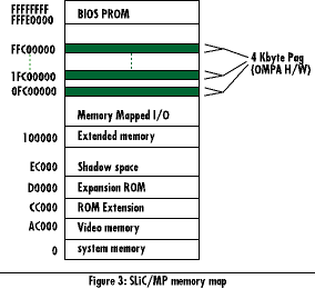 The address map for SLiC/MP hardware resides in the memory-mapped I/O device area in the PC memory map. The SLiC/MP interrupt control module supports 8259-based Programmable Interrupt Controllers (PICs) to achieve PC compatibility in a flexible manner. To achieve symmetry, the hardware interrupt requests are routed to each processor under hardware or software control. Hardware control also involves distributing interrupts in a round-robin fashion. This distribution mechanism ensures that no one processor is burdened with servicing all system interrupts. By basing the system interrupt architecture around the 8259, existing software drivers will be fully compatible with the SLiC/MP architecture without modifications. In addition, since all current uniprocessor chipsets integrate a pair of 8259 PICs as part of the chipsets, developing cost efficient SLiC/MP solutions will be straightforward.
| CPU Architecture | Cache-to-Cache Transfers | Write Allocate | Summary | Page Top | SLiC/MP Inter-Processor Interrupts IPIs are high priority mechanisms used by MP operating systems to allow processors to communicate among themselves. IPIs are generally used tin functions such as starting threads for execution and flushing TLB entries. The SLiC/MP interrupt architecture enables fast and efficient generation, acknowledgment, prioritization and EOI-ing of IPIs. This is achieved via two components: The IPI control block and the IPI vector register. The IPI control block is responsible for dispatch, acknowledgment and End Of Interrupt (EOI) while the IPI vector register is responsible for providing the preprogrammed IPI vector to the appropriate processor. IPIs are higher priority than 8259 interrupts.
IPI Control
Dispatching an IPI
IPI Interrupt Acknowledge Cycle The IPI vector register is a single 8 bit (R/W) register that is part of the SLiC/MP module which used to store the 8 bit interrupt vector associated with IPIs. This vector register is shared between processors and is initialized by the Operating system after bootup. During INTerrupt Acknowledge cycles (INTACK) issued by a processor in response to an IPI, this vector will be provided directly by the SLiC/MP logic without the need for passing the bus cycle to the 8259 PIC. This direct intervention helps achieve higher performance by minimizing the number of I/O cycles it takes to acknowledge the IPI. Traditionally, such I/O cycles would take large number of processor bus cycles due to slow I/O devices on the expansion bus (i.e., ISA, PCI or VL). 8259 Interrupt requests are lower in priority than IPIs. Therefore, if an 8259 interrupt request is issued while an IPI is pending, the IPI will be serviced ahead of the 8259 interrupt (servicing in this case refers to providing the Interrupt Vector). This prioritization holds true even if the 8259 interrupt occurred prior to the IPI. This can occur if the 8259 interrupt request caused the INTRx pin to be asserted, and prior to the interrupted processor generating an INTACK cycle, an IPI is issued to the same processor. In this case, the INTACK cycle will cause the SLiC module to provide the IPI vector directly to the processor instead of allowing the bus cycle to proceed along to the 8259 PIC. The SLiC/MP interrupt architecture achieves high performance, PC compatibility and low cost. In addition, SLiC/MP interrupt architecture is an open solution that enables the development of a variety of desktop MP systems that are CISC or RISC based.
| CPU Architecture | Cache-to-Cache Transfers | Write Allocate | Summary | Page Top | SLiC/MP CPU Architecture SLiC/MP specifications recommend a set of enhancements that increases overall system performance by optimizing the CPU cache and bus architecture for the behavior of MP systems. The goal of these enhancements is to increase bus bandwidth, reduce latencies and minimize 1st level cache misses and associated miss penalties.
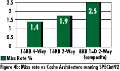
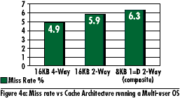
CPU Cache Architecture A number of benchmarks can be used to measure the performance improvements that can be gained by varying the cache architecture. Benchmarks, such as SPECmarks, give a good indication of cache performance when running applications while studies on multitasking Operating Systems (OS) give a good understanding of cache performance under more stringent conditions due to reduced locality. Figure 4a illustrates estimated cache performance of various cache size/associativity when running a multi-user OS under a heavy load and Figure 4b shows the same running SPECmarks. Optimizing for both would improve overall system performance. As expected, the above data indicates that increased associativity and cache size will reduce miss rates and hence improve performance (assuming equivalent miss penalties). Unified caches exhibit higher hit rate (lower miss rate) than separate Instruction and Data caches due to dynamic date/code allocation. The next step after minimizing miss rates is to minimize miss penalty.
| CPU Architecture | Cache-to-Cache Transfers | Write Allocate | Summary | Page Top | SLiC/MP Cache-to-Cache Transfers Supporting cache to cache transfers in SLiC/MP systems reduces cache miss penalties as well as improve bus bandwidth. This is achieved by providing the critical word requested by a processor (requester), which has been modified by another processor (owner), directly from the owner. Special control logic on processors is needed to allow for this type of operation to occur. Figure 5 shows the performance degradation associated with cache misses and the advantage of cache-to cache transfers. The performance degradation is based on the following system assumptions.
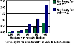 Figure 5 shows the performance degradation (in penalty CPU Cycles Per Instructions-CPI) that is incurred when a cache-to cache (C2C) condition arises as a function of frequency of occurrence. A cache-to-cache condition occurs when a miss in the 1st level cache of a second processor that had modified that line (owner). Under these circumstances, current processors cause the requesting the processor to ignore the current operation, the owning processor to perform a write back cycle followed by the requesting processor restarting the operation, which causes a substantial miss penalty. Cache-to-Cache transfers from the owner's first level cache to the requester's first level cache dramatically minimizes this miss penalty in addition to improving overall bus bandwidth. Even under the lowest probability of occurrence in the graph (0.5%) the miss penalty of not supporting cache to cache is 0.14 CPI (cycles per instruction). This is calculated as follows
14 cycles/miss x 0.5%=0.07 bus CPI Assuming 2:1 core to bus clock ratio -> Penalty =0.07 x 2=o.14 CPI
Considering current high performance superscalar processors can achieve 2 instructions/cycle (or 0.5 CPI) a miss rate of 0.14 CPI is equivalent to a 28% performance degradation (0.14/0.5=.28) which is substantial. Next generation processors are attempting to achieve even more throughput and hence lower CPIs (less than 0.5) which makes miss penalties costlier.
| CPU Architecture | Cache-to-Cache Transfers | Write Allocate | Summary | Page Top | SLiC/MP Write Allocate Supporting Write Allocate is also recommended is SMP systems. Write Allocate allows a line to be allocated when a 1st level cache miss occurs on a write operation to a cacheable region. The advantage of write allocate is that subsequent references to that same line would not miss in their 1st level cache since it was allocated. Code locality indicates that when a data is referenced there is a high probability that adjacent data will be referenced as well. Since there is a high probability that the same or adjacent data will be referenced, allocating on writes will improve performance by eliminating the 1st level cache miss.
Read with Intent to Modify
| CPU Architecture | Cache-to-Cache Transfers | Write Allocate | Summary | Page Top | Summary of the SLiC/MP Abstract The SLiC/MP architecture enables the development of high performance desktop SMP systems. The architecture covers an open interrupt architecture specification as well as providing a set of recommendations for optimizing processors to SMP desktop systems. These recommendations enable the development of high performance machines around off-the-shelf components which dramatically reduces system cost. SLiC/MP architecture can be used to build a variety of systems CISC, or RISC, based and achieve HAL/Microkernel level compatibility.
Bibliography
|